← Step By Step New Racing Cdi Box Wiring Diagram Instructions For Upgrading Your Standard Cdi System Today - How to wire a 6 pin racing cdi: complete diagram guide Simplify Your Next Electrical Repair Project With A Clear Ford Escort Wiring Diagram And Troubleshooting Schematic Manual - 1989 ford escort electrical and vacuum troubleshooting manual original →
If you are searching about What Is A 4-Layer PCB?-ucreatepcb.com you've came to the right web. We have 35 Pics about What Is A 4-Layer PCB?-ucreatepcb.com like Essential PCB Design Rules for Minimizing Crosstalk and EMI, PCB Design Rules - ElectronicsHacks and also 4 Layer Flex PCB: Design and Manufacturing Guide- Jarnistech. Here it is:
What Is A 4-Layer PCB?-ucreatepcb.com
 www.ucreatepcb.com
What Is A 4-Layer PCB?-ucreatepcb.com
PCB Design Rules For Wiring And Crosstalk – PCB HERO
 www.pcb-hero.com
PCB Design Rules For Wiring And Crosstalk – PCB HERO
6 Common PCB Design Rules
 www.diskmfr.com
6 Common PCB Design Rules
How To Design A 4-layer PCB - PCBA Manufacturers
 www.pcba-manufacturers.com
How to design a 4-layer PCB - PCBA Manufacturers
2 Layer Pcb Design Guidelines - Design Talk
 design.udlvirtual.edu.pe
2 Layer Pcb Design Guidelines - Design Talk
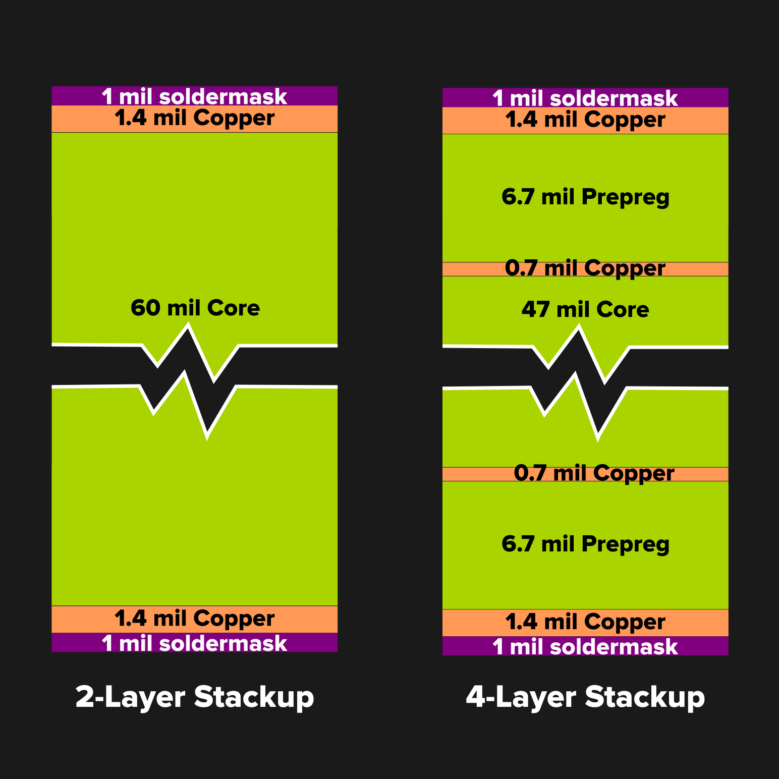
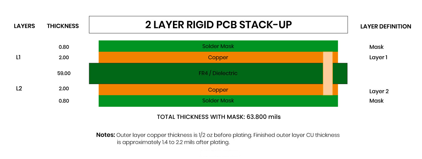
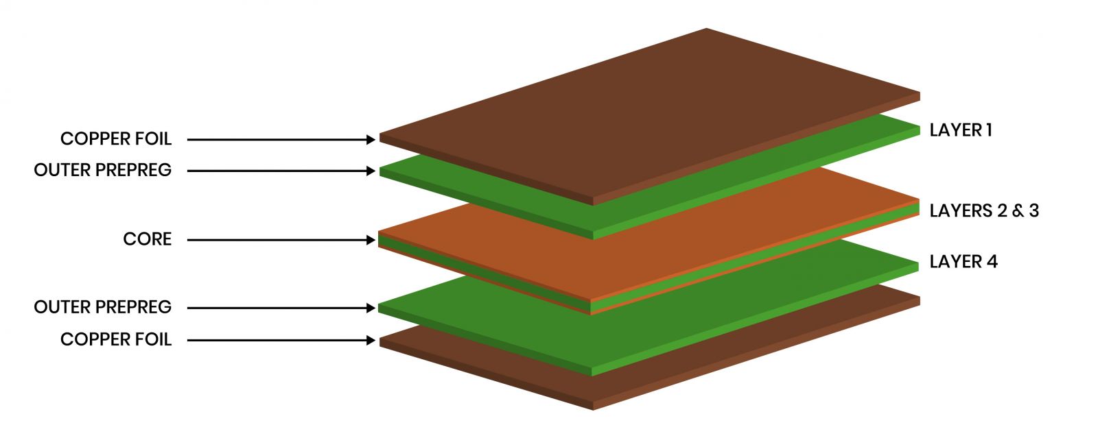
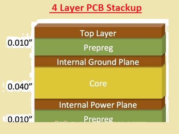
PCB Stack-Up Guide & Examples | San Francisco Circuits
 www.sfcircuits.com
PCB Stack-Up Guide & Examples | San Francisco Circuits
A Comprehensive Guide About 4 Layer PCB Stack Up
 www.elepcb.com
A Comprehensive Guide About 4 Layer PCB Stack Up
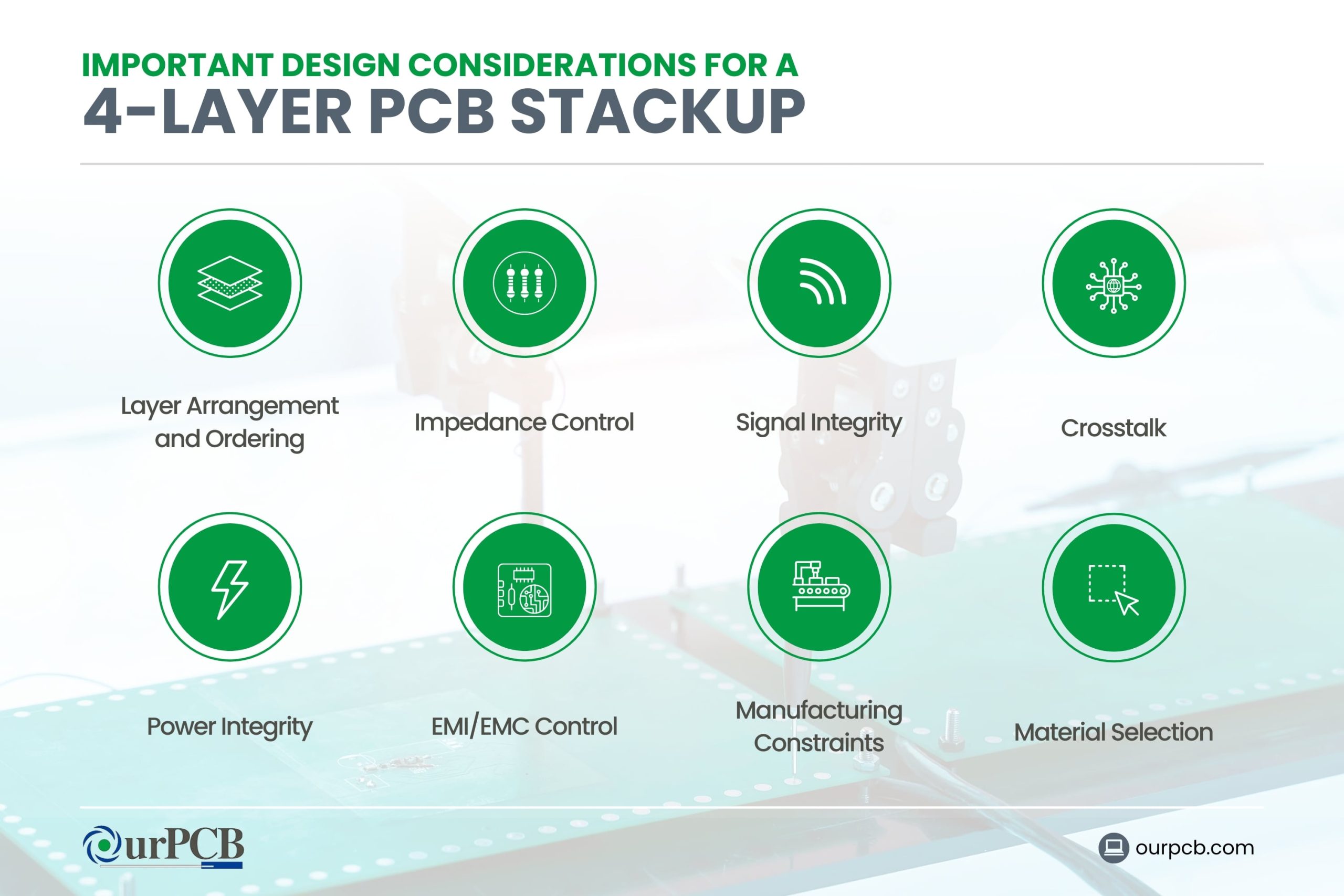
4-Layer PCB Design Guidelines: Key Tips For Success | Viasion
 www.viasion.com
4-Layer PCB Design Guidelines: Key Tips for Success | Viasion
4-Layer PCB Design Strategies - VSE
 www.vse.com
4-Layer PCB Design Strategies - VSE
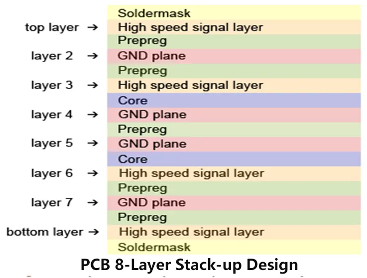
FPGA/SoC + DDR PCB Design Rules: Basic Guidelines You Need To Know
 www.raypcb.com
FPGA/SoC + DDR PCB Design Rules: Basic Guidelines You need to Know ...
PCB Stack-Up Guide & Examples | San Francisco Circuits
 www.sfcircuits.com
PCB Stack-Up Guide & Examples | San Francisco Circuits
PCB Design Rules And Guidelines » Hackatronic
 hackatronic.com
PCB Design Rules and Guidelines » Hackatronic
4-Layer PCB Design Guidelines: Key Tips For Success | Viasion
 www.viasion.com
4-Layer PCB Design Guidelines: Key Tips for Success | Viasion
PCB Stack-Up Guide & Examples | San Francisco Circuits
 www.sfcircuits.com
PCB Stack-Up Guide & Examples | San Francisco Circuits
PCB Stack-Up Guide & Examples | San Francisco Circuits
 www.sfcircuits.com
PCB Stack-Up Guide & Examples | San Francisco Circuits
Essential PCB Design Rules For Minimizing Crosstalk And EMI
 greatpcb.com
Essential PCB Design Rules for Minimizing Crosstalk and EMI
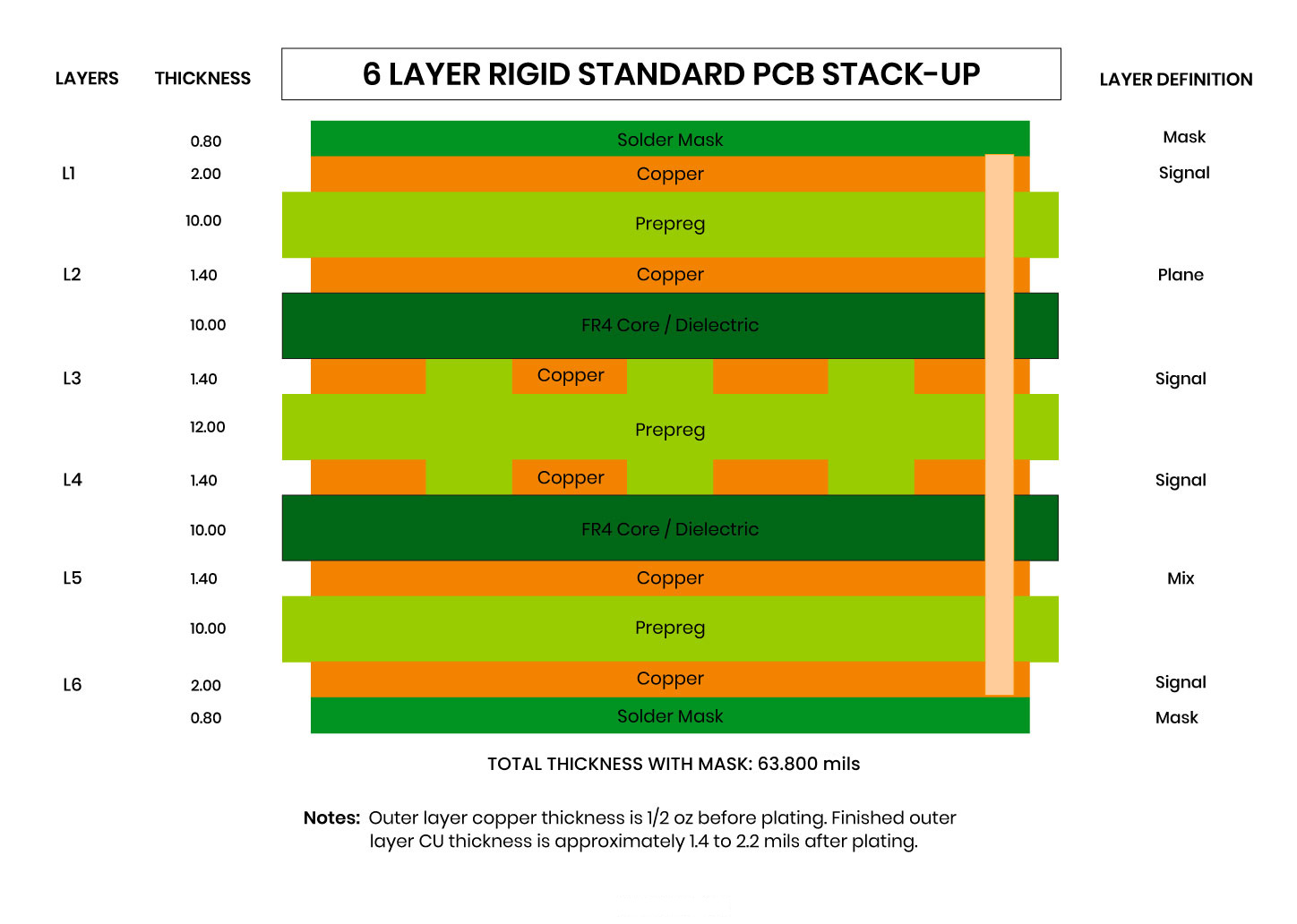
PCB Layer Stack Up And Rules To Properly Design - Jarnistech
 www.jarnistech.com
PCB Layer Stack Up and Rules to Properly Design - Jarnistech
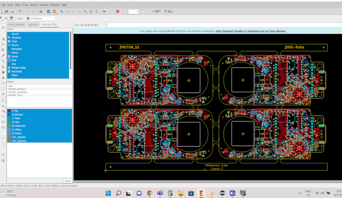
PCB Review Request! My First 4-Layer PCB Design : R/PrintedCircuitBoard
 www.reddit.com
PCB Review Request! My first 4-Layer PCB design : r/PrintedCircuitBoard
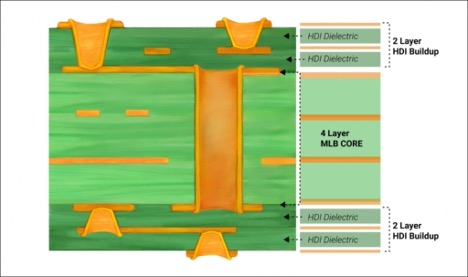
PCB Stack-up Design Rules - Zuken US
 www.zuken.com
PCB Stack-up Design Rules - Zuken US
4 Layer PCB Design Guide: Stackups & Best Practices - GlobalWellPCBA
 www.globalwellpcba.com
4 Layer PCB Design Guide: Stackups & Best Practices - GlobalWellPCBA
An Overview Of Layer Stack Management In PCB Design, 44% OFF
 www.oceanproperty.co.th
An Overview Of Layer Stack Management In PCB Design, 44% OFF
Key Points In The Design Of 4 Layer PCB | Viasion
 www.viasion.com
Key Points in the Design of 4 Layer PCB | Viasion
Do 2 Or 4 Layer Pcb Design By Venky_8896 | Fiverr
 www.fiverr.com
Do 2 or 4 layer pcb design by Venky_8896 | Fiverr
Ten Golden Rules Of PCB Design & Its Guidelines - AES
 absolutepcbassembly.com
Ten Golden Rules of PCB Design & its Guidelines - AES
4-Layer PCB Design Guidelines: Key Tips For Success | Viasion
 www.viasion.com
4-Layer PCB Design Guidelines: Key Tips for Success | Viasion
PCB Design Rules - ElectronicsHacks
 electronicshacks.com
PCB Design Rules - ElectronicsHacks
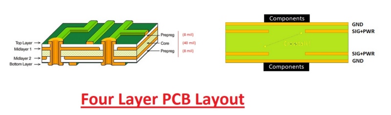
Four Layer PCB Layout: Design Process And Cost Of Manufacturing
 www.theengineeringknowledge.com
Four Layer PCB Layout: Design Process and Cost of Manufacturing
PCB Review Request! My First 4-Layer PCB Design : R/PrintedCircuitBoard
 www.reddit.com
PCB Review Request! My first 4-Layer PCB design : r/PrintedCircuitBoard
PCB Review Request! My First 4-Layer PCB Design : R/PrintedCircuitBoard
 www.reddit.com
PCB Review Request! My first 4-Layer PCB design : r/PrintedCircuitBoard
Basic Rules Of PCB Design For High-Quality Circuit Boards
 hilelectronic.com
Basic Rules of PCB Design for High-Quality Circuit Boards
4-Layer PCB Design Guidelines: Key Tips For Success | Viasion
 www.viasion.com
4-Layer PCB Design Guidelines: Key Tips for Success | Viasion
What Is The Better PCB: 2 Layer Vs 4 Layer PCB?
 www.pcbmay.com
What Is the Better PCB: 2 Layer vs 4 Layer PCB?
Master The Top 7 PCB Design Rules For Successful Layouts
 unitypcb.com
Master the Top 7 PCB Design Rules for Successful Layouts
What Is A 4-Layer PCB Stackup? Examples & Guidelines
 www.ourpcb.com
What is a 4-Layer PCB Stackup? Examples & Guidelines
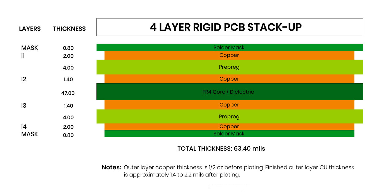
4 Layer Flex PCB: Design And Manufacturing Guide- Jarnistech
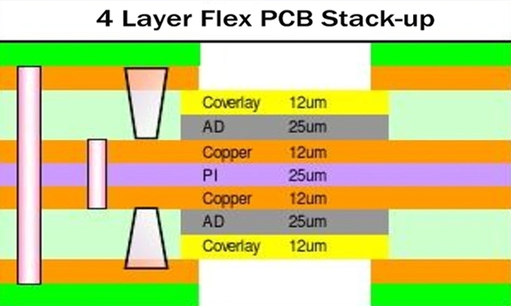 www.jarnistech.com
4 Layer Flex PCB: Design and Manufacturing Guide- Jarnistech
How to design a 4-layer pcb. Pcb design rules for wiring and crosstalk – pcb hero. Fpga/soc + ddr pcb design rules: basic guidelines you need to know ...