← Why Following A 6 Volt Ford 8n Wiring Diagram Is Crucial For Proper Ignition On Your Antique Ford Tractor - 8n wiring diagram 6 volt Mastering Your Small Engine Electrical System With A 5 Wire Rectifier Wiring Diagram And The Essential Rly0 Wiring Schematic - Understanding the 3 wire rectifier diagram: a detailed guide →
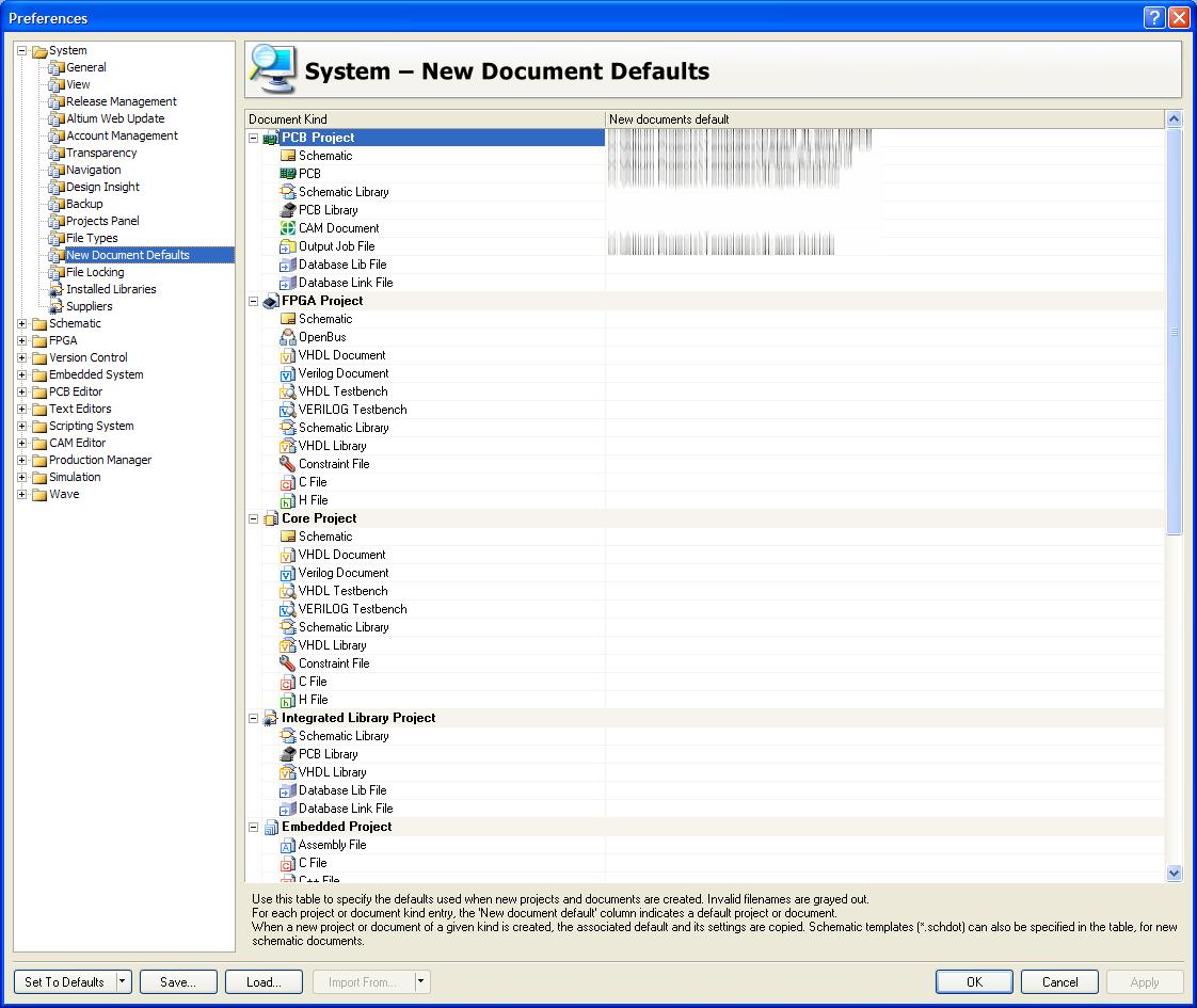
If you are looking for Getting Started with Harness Design in Altium Designer 25 | Altium you've came to the right place. We have 27 Pics about Getting Started with Harness Design in Altium Designer 25 | Altium like Managing Pad & Via Templates using the PCB Panel in Altium NEXUS, Relay Wiring Diagram Template and also Altium Designer Tutorial 38: How to create PCB Template in Altium. Read more:
Getting Started With Harness Design In Altium Designer 25 | Altium
 resources.altium.com
Getting Started with Harness Design in Altium Designer 25 | Altium
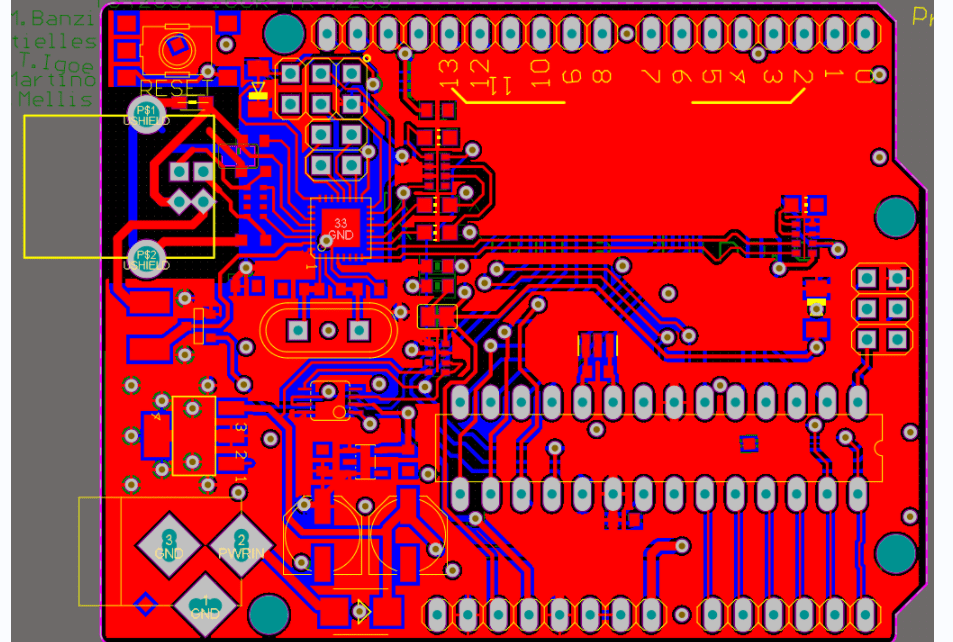
Altium Count Number Of Selected Vias - Electrical Engineering Stack
 electronics.stackexchange.com
Altium count number of selected vias - Electrical Engineering Stack ...
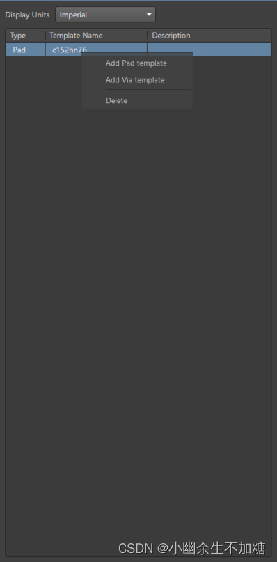
Managing Pad & Via Templates Using The PCB Panel In Altium NEXUS
 www.altium.com
Managing Pad & Via Templates using the PCB Panel in Altium NEXUS ...
Defining The Wiring Diagram | Altium Designer Technical Documentation
 www.altium.com
Defining the Wiring Diagram | Altium Designer Technical Documentation
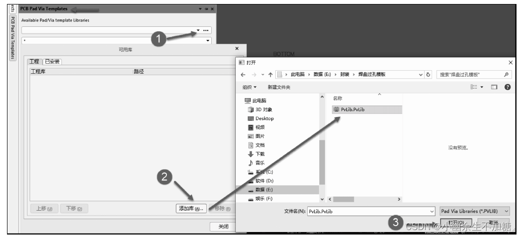
使用焊盘过孔模板 | Altium Designer 25 技术文档
 www.altium.com
使用焊盘过孔模板 | Altium Designer 25 技术文档
Short Circuit Detector Schematic » Wiring Diagram
 www.organised-sound.com
Short Circuit Detector Schematic » Wiring Diagram
使用焊盘过孔模板 | Altium Designer 25 技术文档
 www.altium.com
使用焊盘过孔模板 | Altium Designer 25 技术文档
How To Import Altium Designer PCB Board In KiCad? — RefCircuit
 refcircuit.com
How to import Altium Designer PCB board in KiCad? — RefCircuit
Altium Template Folder | Create A Altium Schematic – FJCY
 mateamilojkovic.com
Altium Template Folder | Create A Altium Schematic – FJCY
Altium PCB Templates: A Comprehensive Guide For Beginners – Hillman
 hillmancurtis.com
Altium PCB Templates: A Comprehensive Guide for Beginners – Hillman ...
|Altium| PCB-Template - Mikrocontroller.net
 www.mikrocontroller.net
|Altium| PCB-Template - Mikrocontroller.net
AD21 PCB设计的高级应用(七)盲埋孔的设置_ad盲孔怎么设置-CSDN博客
 blog.csdn.net
AD21 PCB设计的高级应用(七)盲埋孔的设置_ad盲孔怎么设置-CSDN博客
Lötpaste Einfach Erklärt: Was Sie Ist, Wie Man Sie Verwendet Und Wie
 www.fastturnpcbs.com
Lötpaste Einfach Erklärt: Was Sie Ist, Wie Man Sie Verwendet Und Wie ...
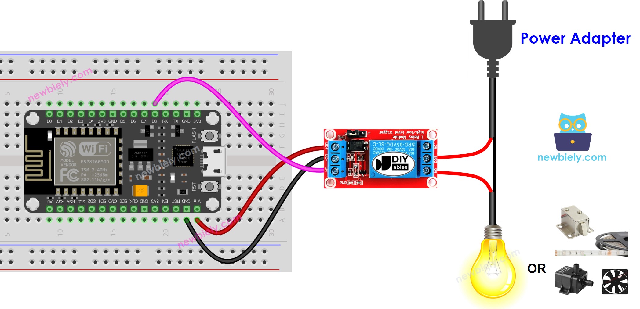
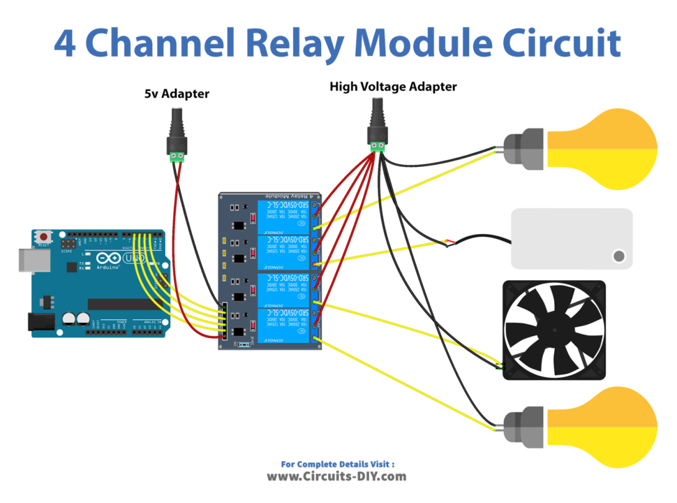
ESP8266 - Controls Relay Via Web | ESP8266 Tutorial
 newbiely.com
ESP8266 - Controls Relay via Web | ESP8266 Tutorial
Altium PCB Templates - Effektiver Arbeiten | Altium
 resources.altium.com
Altium PCB Templates - Effektiver Arbeiten | Altium
Altium Designer Tutorial 38: How To Create PCB Template In Altium
 www.youtube.com
Altium Designer Tutorial 38: How to create PCB Template in Altium ...
AD21 PCB设计的高级应用(七)盲埋孔的设置_ad盲孔怎么设置-CSDN博客
 blog.csdn.net
AD21 PCB设计的高级应用(七)盲埋孔的设置_ad盲孔怎么设置-CSDN博客
RF PCBにおけるバランとは何か、そしてそれが必要か? | ブログ | Altium
 resources.altium.com
RF PCBにおけるバランとは何か、そしてそれが必要か? | ブログ | Altium
How To Plan PCB Projects From Design To Examples ? - RayPCB
 www.raypcb.com
How to Plan PCB Projects from Design to Examples ? - RayPCB
ハーネスの製造図面の作成 | Altium Designer 技術文書
 www.altium.com
ハーネスの製造図面の作成 | Altium Designer 技術文書
Overview Guide: Relays – Device Help
 install.verizonconnect.com
Overview guide: Relays – Device Help
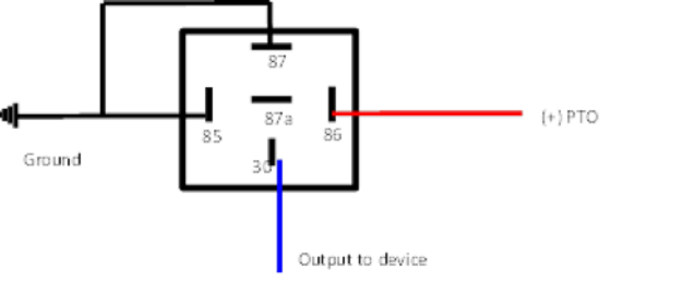
All About Vehicle Electrical Relays
 www.onallcylinders.com
All About Vehicle Electrical Relays
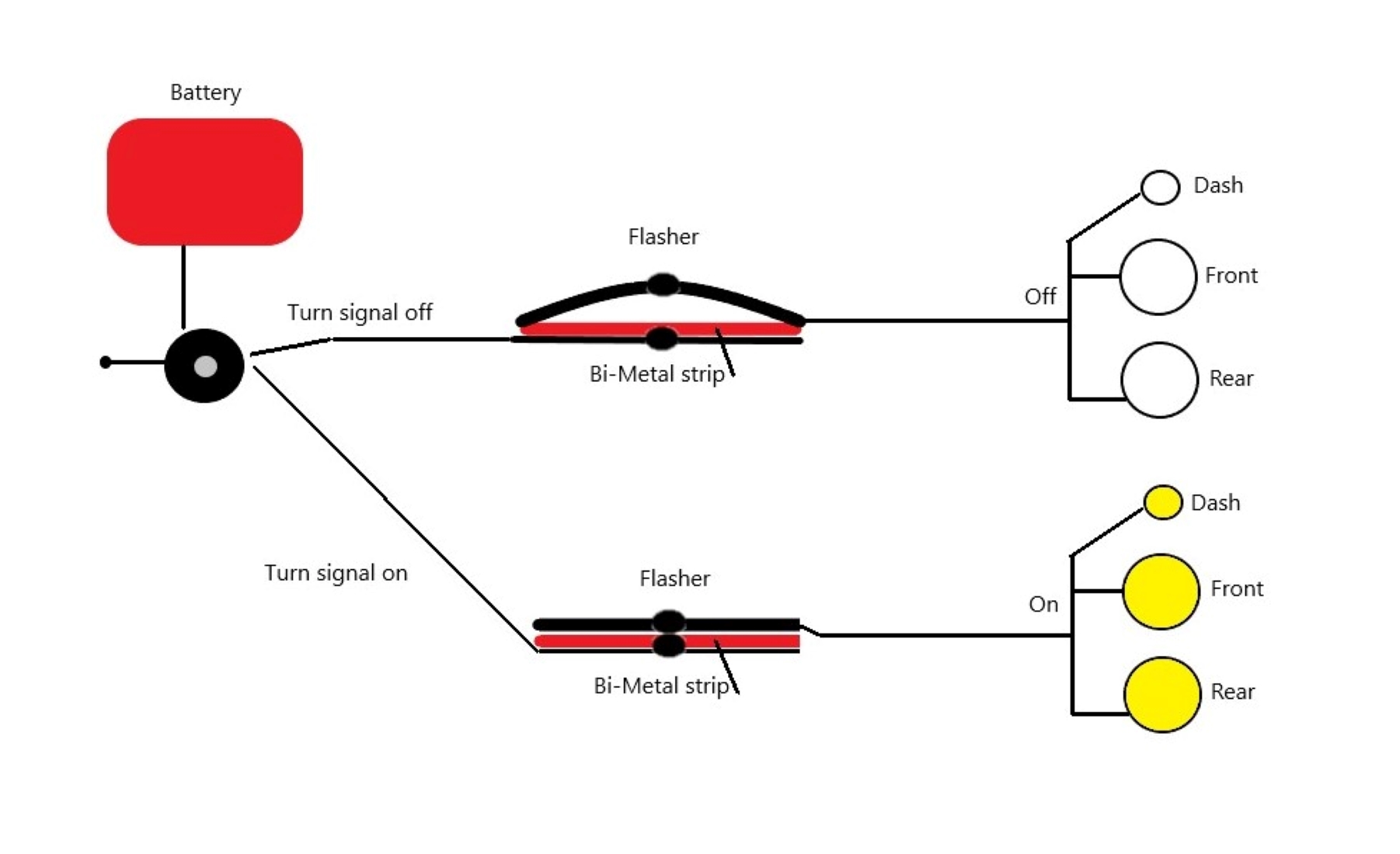
Relay Wiring Diagram Explained
 www.wiringdraw.com
Relay Wiring Diagram Explained
Defining The Wiring Diagram | Altium Designer Technical Documentation
 www.altium.com
Defining the Wiring Diagram | Altium Designer Technical Documentation
How To Make A Small Relay Switch At Mary Lockridge Blog
 storage.googleapis.com
How To Make A Small Relay Switch at Mary Lockridge blog
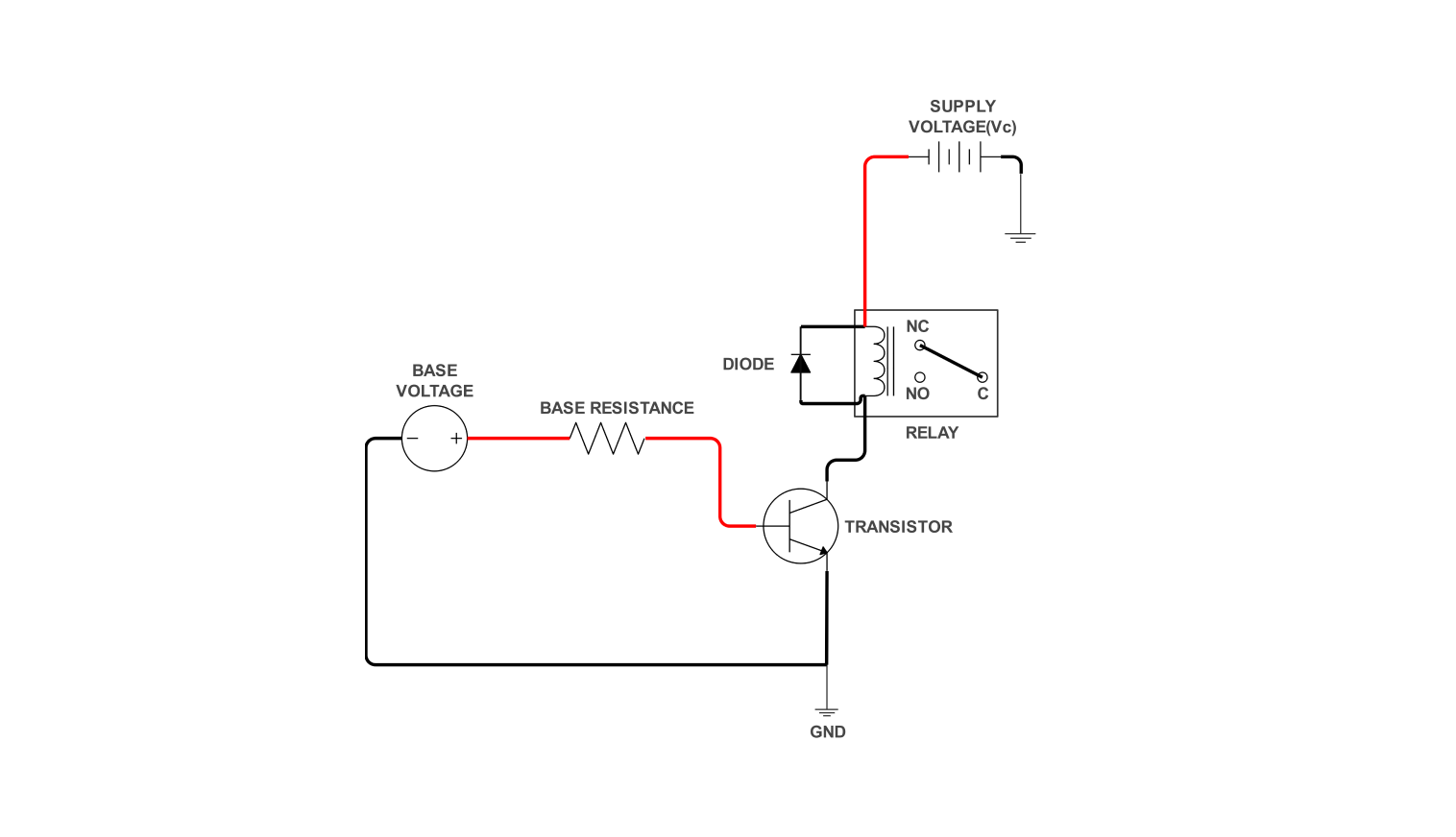
Relay Wiring Diagram Template
 edrawmax.wondershare.com
Relay Wiring Diagram Template
Wiring Diagram Of Relay Switch - Wiring Digital And Schematic
 www.wiringdigital.com
Wiring Diagram Of Relay Switch - Wiring Digital and Schematic
Altium template folder. Ad21 pcb设计的高级应用(七)盲埋孔的设置_ad盲孔怎么设置-csdn博客. Managing pad & via templates using the pcb panel in altium nexus ...